Description
[vc_widget_sidebar sidebar_id=”mmpm_menu_widgets_area_1″]
Key Features
- Superior dual detector technology (digital image chain and active temperature-stabilized digital detector with 30 fps) for brilliant live images
- High magnification
- Precise Manipulation
- High repeatability
- 180 kV / 15 W high-power open nanofocus tube with up to 200 nanometer detail detectability
- Upgradeable to nanoCTÒ
- Optional:
- x|act software package for easy and fast CAD based high-resolution automated X-ray inspection (μAXI) for extremely high defect coverage with high magnification and repeatability
- Brilliant live inspection images due to high dynamic temperature-stabilized digital GE DXR detector with 30 fps (frames per second) and active cooling
- 3D computed tomography scans within 10 seconds
- Up to 2 times faster data acquisition at the same high image quality level by diamond|window
Customer Benefits
- Combined 2D / 3D CT operation
- Superior dual detector technology (digital image chain and active temperature-stabilized digital detector with 30 fps) for brilliant live images
- Automation of inspection steps possible
- Outstanding ease-of-use
Applications
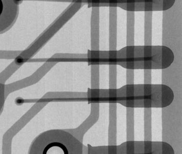
Mounted Printed Circuit Boards
nanofocus X-ray image of flip- chip solder joints inside a processor case. The image shows one solder bridge and several open solder joints. The solder joint diameter is app. 150 µm. (Learn More)
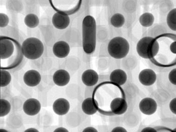
Semiconductor and Other Electronic Components
nanoCT® of a µBGA after 4000 temperature stress cycles. Due to a voxelsize of 0.5 microns, cracks with 8 to < 1 micron are detectable. (Learn More)
Accessories
- CT option: includes software datos|x, high precision rotation unit, reconstruction and visualization workstation
- quality|review: Repair station software for visualizing and manual review of results from an automatic program run, e.g. bga|module, qfp|module or vc|module.
- converter:Software package to convert result files, generated by quality|assurance or x|act, into other formats, required by third party software.
- quality|analyst: Software package for analyzing and visualizing inspection results, which are collected by an automatic program and reviewed with quality|review.
- diamond|window: up to 2 times faster data acquisition at the same high image quality level
- 4″ Image Intensifier with 4MP Image Chain: This high resolving 4’’ Image Intensifier image chain: with full digital read out and image processing is a basic part for all high quality phoenix|x-ray 2D systems. The detector is suitable for 2D real time inspection.
Specifications
| Max. tube voltage | 180 kV |
|---|---|
| Max. output | 15 W |
| Detail detectability | Up to 0,2 µm |
| Min. focus-object-distance | 0.3 mm |
| Max. voxel resolution (depending on object size) | < 1 µm |
| Geometric magnification (2D) | Up to 1970-fold |
| Geometric magnification (3D) | <300-fold |
| Max. object size (height x diameter) | 680 mm x 635 mm / 27″ x 25″ |
| Max. object weight | 10 kg/ 22 lbs |
| Image chain | 2 megapixel digital image chain |
| Manipulation | 5-axis sample manipulation |
| 2D X-ray imaging | yes |
| 3D computed tomography | yes (optional) |
| System size | 1860 mm x 2020 mm x 1920 mm / 73.2” x 79.5” x 75.6” |
| System weight | 2600 kg / 5732 lbs |
| Radiation Safety | – Full protective radiation safety cabinet according to the German RöV (attachment 2 nr. 3) and the US Performance Standard 21 CFR 1020.40 (Cabinet X-ray Systems) – Radiation leakage rate: < 1.0 µSv/h measured 10 cm from cabinet wall |
Download
| Descriptions | English | Deutsch | RU | Español |
|---|---|---|---|---|
| 2D and USB flash device evaluation with high resolution X-ray inspection and CT German Paper in PLUS | ||||
| Diamond Window Brochure | ||||
| Inspection Technologies Brochure | ||||
| nanome|x / microme|x DXR | ||||
| Package Brochure | ||||
| PCBA Brochure | ||||
| x-act Brochure |